Realtime Audio DSP with the STM32F4
ADC -> DSP -> DAC Example
Written by Ross Wolin - last updated 2014.01.19
Introduction

This project creates a chain which:
- Converts a continous analog signal to a stream of discrete digital samples, using an ADC
- Runs each sample through a DSP function: in this example, the DSP is a simple notch filter
- Converts the resulting stream of discrete digital samples to an continuous analog voltage using a DAC
Build Environment: This project was built on Ubuntu Linux 12.04 LTS, compiled with GNU Tools for ARM Embedded Processors 4.8-2013q4, and programmed into an STM32F4 Discovery Kit using the 2014.01.18 commit of STLINK. If you need to install and set up the toolchain, refer to my previous blog posting: STM32 Discovery Development on Linux
Download ADC_DSP_DAC Example and STM32 Libraries
The project files are hosted on Github, you can clone the repository with:
cd ~
git clone https://github.com/rowol/adc_dsp_dac
The ADC_DSP_DAC example source is now in ~/adc_dsp_dac/project
I have also included a STM's library source, needed to build the project, in the ~/adc_dsp_dac/STM32F4-Discovery_FW_V1.1.0 directory. If you want the complete STM library, utility, and examples source code, download that from STM's website
If you don't wish to clone the repository with Git, you may also retreive the project
as a zipfile.
Building the Code
Build the code by running:
make
Program the STM32F4 Discovery with STLINK by running:
make burn
How the Code Works
The STM32F4 can do all sorts of fancy things with the ADCs, like making the ADCs run continuously and store the results with DMA, generating an interrupt when a conversion is complete, etc. In our realtime DSP application we would like to process each ADC sample when it's available, so we disable the ADC continuous conversions, DMA, and interrupts, and run the ADC in single-shot mode.
In the adc.c::ADC_init() function ADC1 channel 15 is set up in single-shot mode with all DMA and interrupt features disabled. The ADC does a conversion when you tell it do by calling ADC_SoftwareStartConv() and sets a flag, which you can monitor with ADC_GetSoftwareStartConvStatus() to determine when the conversion is complete.
I'm running the ADC with a divided by 8 clock to reduce the 84Mhz APB2 clock down to 10.5Mhz so it falls into the 600Khz-30Mhz range allowed for the ADC clock in the STM32F4 datasheet. I have also set the sampling time (how long the ADC "measures/averages" the signal before starting a conversion) to 144 cycles. Assuming the ADC takes about 16 cycles for a conversion, this means sampling+conversion will take about 160 cycles or 15.2uS with our 10.5Mhz ADC clock. Our timer interrupt generated sampling rate of 44Khz gives us 22.7uS between samples, so there is plenty of time for the ADC conversion to complete between each sample. The 44Khz sampling rate was chosen because the Nyguist-Shannon sampling theorem states you want to sample at twice the highest frequency in your input signal: audio CDs are sampled at approximately 44Khz.
DAC2 is also configured with DMA disabled. When you write to the DAC with dac.c::DAC2_set(), it changes the DAC2 value using the DAC_SetChannel2Data() library function.
In the tmr_sample module, the tmr_sample::tmr_sample_init() function configures basic timer TIM6 to generate interrupts at a rate of 44Khz, meaning main::TIM6_DAC_IRQHandler() is called approximately every 22.7uS. This IRQ handler does a couple of things:
- ADC1 conversion is read via the adc.c::ADC_get() function, and a new conversion is started by calling adc.c::ADC_start()
- The sample read from ADC1 is digitally filtered, using the main.c::filter() function
- The filtered result is written to DAC2, with the dac.c::DAC2_set() function
- Additionally, the PC.4 output pin is toggled every 25 calls, at a rate of 880Hz (this is used to generate a square wave for testing/illustration)
My example simple digital filter is a notch filter with the peak centered at 880Hz. The graph shows the response from 0Hz to 5500Hz, with unity gain at the top of the peak. I designed this filter with FIVIEW, using the command "fiview 44000 -i BpRe/50/880"

IO Pin Summary
- PC.4 is configured as a GPIO output
- ADC1 channel 15 is connected to PC.5 input
- DAC2 is connected to the PA.5 output
Testing
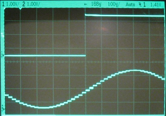
By connecting PC.4 to PC.5 with a jumper, you can run an 880Hz square wave into the ADC, through the digital filter, out the DAC, and observe the results with an oscillscope at PA.5. Square waves are composed of a sequence of sine waves of the fundamental plus odd harmonics: running a square wave through a good notch filter centered around the fundamental frequency will yield a sine wave.
These events happen in our project with PC.4 jumpered to PC.5:
- The IRQ handler generates an 880Hz square wave by toggling an IO pin every 25 calls (i.e. 44Khz/25/2 = 880Hz
- This square wave is sampled by the ADC.
- The result is run though the digital notch filter, removing all the component sine waves except the fundamental (first) harmonic at 880Hz, so the resulting filtered waveform is a sine wave.
- The filtered sine wave result is written to the DAC which converts it back to an analog waveform.


Development Kit Hardware
The STM32F4 Discovery is a $15 development board, featuring a 168Mhz ARM Cortex M4 (STM32F407VGT6) The ARM is programmed via an STLINK/V2 interface connected to a PC's USB port (i.e. requires no JTAG plug, ICD, BDM, proprietary dongle, etc.)
Links
- STM32F4 Discovery Kit Resource Page
- CMSIS - Cortex Microcontroller Software Interface Standard
- FIVIEW - A Digital Filter Design, Viewing, and Comparison Tool
Send comments, questions, money in large denominations, etc to eng at mysticengineering.com
If you enjoyed this article, please consider buying my products ...

|

|
|
ATX PS Adapter
Use an ATX PC power supply as a 5V, 3.3V, and +12V/-12V bench supply the easy way, without cutting the case or mounting external connectors, resistors, LEDs, switches, and fuses. Provides visual indication when supply is plugged in and turned on, also fuses the power voltage outputs for safety. Run USB powered development boards via the USB connectors on the 5V line. |
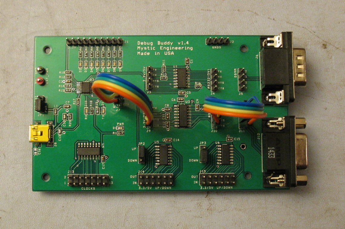
Ultimate Serial Port (Debug Buddy)
USB serial port with standard, 5V and 3V RS232, plus integrated null modem and gender changer. Implements TX/RX and RTS#/CTS# for optional hardware handshake. Also includes 3.3V<->5V level shifters, debug LEDs, and 13 clock sources. Valuable tool for hands on problem solving and hacking |

